Huawei says it has found a new route around the limits of advanced lithography, but the claim is still a roadmap, not proof that China has solved leading-edge chip manufacturing.
Huawei grabbed the chip industry's attention this week by presenting the Tau Scaling Law, a new framework the company says can help it reach transistor density equivalent to a 1.4-nanometer process by 2031. The point is not that Huawei has suddenly caught TSMC, Intel, or Samsung. It has not. The point is that Huawei is trying to change the terms of the race at a moment when US export controls are built around denying China access to the most advanced lithography tools.
According to Huawei's May 25 announcement from the 2026 IEEE International Symposium on Circuits and Systems in Shanghai, He Tingbo, chair of the Huawei Scientist Committee and president of its semiconductor business department, described Tau Scaling as a shift from pure geometric shrinking toward compressing signal propagation time across devices, circuits, chips, and systems. That sounds abstract, but the commercial message is clear: if Huawei cannot rely on ASML's extreme ultraviolet machines, it wants to make chips denser and faster through architecture, stacking, interconnects, and tighter system design.
What LogicFolding is meant to do
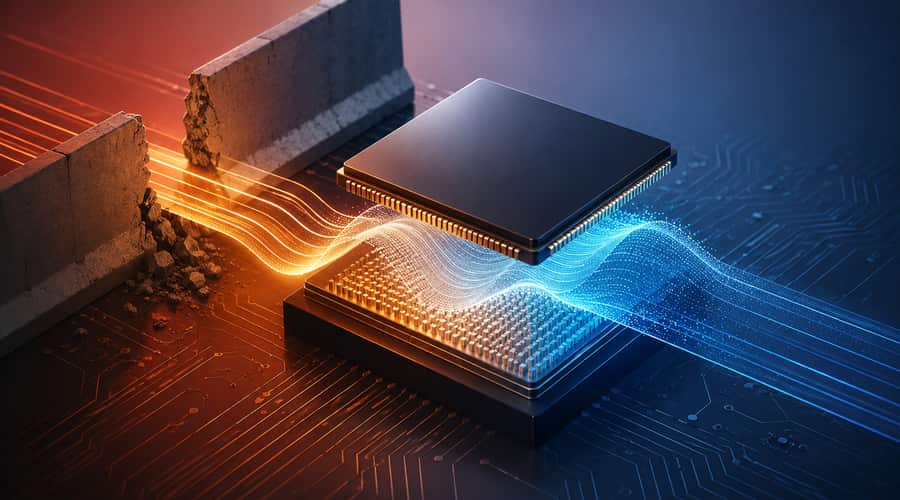
The most important piece of the announcement is LogicFolding, a chip architecture Huawei says will shorten wiring paths and reduce resistive and capacitive load inside chips. Instead of treating progress as a simple matter of making every transistor smaller, the company is trying to raise effective density by reorganizing how logic is laid out and connected.
Huawei says it has designed and mass-produced 381 chips over the past six years using ideas tied to Tau Scaling, serving areas that include smartphones and AI computing. The first Kirin chips scheduled to use LogicFolding are expected in Fall 2026, which makes the coming phone cycle a useful test of how much of this is engineering substance and how much is conference-stage ambition.
The claimed gains are not modest. Reports on Huawei's presentation say LogicFolding could raise transistor density by 55% and improve power efficiency by 41% compared with traditional flat designs. If those numbers survive contact with shipping silicon, they would matter. Smartphones are power-constrained, AI accelerators are heat-constrained, and both markets reward any design that can do more work without demanding a cleaner lithography path than China currently has.
The AI angle is why this story travels beyond semiconductors. Huawei has already been pushing its Ascend line as a domestic alternative to Nvidia chips inside China, where export controls have limited access to the most capable US accelerators. Earlier this year, Huawei also promoted the Atlas 350 accelerator with an Ascend 950PR chip, claiming far higher FP4 performance than Nvidia's China-focused H20 in certain inference workloads. Those comparisons are difficult to verify cleanly because precision formats and software ecosystems differ, but they show where Huawei is aiming: not just phone chips, but the data center stack that powers large AI models.
The caveats are not small
The first caveat is that equivalent density is doing a lot of work here. A chip with density comparable to a 1.4-nanometer process is not the same thing as a chip manufactured on a true 1.4-nanometer node. That distinction matters because process technology brings benefits in power, performance, yield, and device behavior that architectural tricks do not automatically reproduce.
Huawei's manufacturing path is still constrained. Its key domestic foundry partner, SMIC, does not have access to the most advanced EUV lithography systems, and pushing older deep ultraviolet tools through complex multi-patterning raises cost and yield pressure. Analysts have repeatedly warned that moving beyond 7nm-class production without EUV is possible in narrow cases, but difficult to scale efficiently.
Thermals are the other problem. Folding or stacking logic can shorten signal paths, but it can also make heat harder to remove. That matters less in a slide deck than it does in an AI training cluster running under sustained load for days. A dense chip that throttles under pressure is not the same thing as a usable advantage.
DGA Group's Paul Triolo put the limitation clearly in comments cited by CNBC, saying a stacked or folded design can create effective density gains, but it does not solve the full process, yield, power, thermal, and device-performance problems associated with true 1.4nm-class manufacturing. That is the right frame. Huawei may be changing the route, but it has not removed every obstacle on the route.
What to watch next
The 2031 target is useful, but it is not the immediate test. The real signal will come from the first Kirin chips using LogicFolding in Fall 2026. If those chips deliver visible gains in battery life, sustained performance, and production volume, the assumption that China is permanently stuck at 7nm-class capability will look weaker.
Washington should also be watching the system-level story. Export controls have focused heavily on the manufacturing equipment bottleneck, especially EUV machines. Huawei's announcement is a reminder that chip competition does not happen only at the transistor level. Packaging, architecture, software, interconnects, and workload-specific design can all narrow gaps when direct access to leading-edge tools is blocked.
That does not mean Huawei has rewritten chip physics. It means the company is trying to make the blockade less decisive by finding performance elsewhere. The next year will show whether LogicFolding is a real engineering lever or just a clever name for a hard problem. Either way, the semiconductor contest is becoming less about one machine and more about the full stack around it.
Also read: Claude Code and OpenClaw turned AI agents into tech's new force • Polymarket’s whale problem is testing prediction market trust • Universal and TikTok make AI music a licensing issue