Lam Research is pushing AI deeper into the machines that make advanced chips. The bet is that better sensor data inside fab tools can help customers catch defects earlier, lift yields, and squeeze more supply out of expensive manufacturing lines.
Lam Research is no longer just selling equipment into the AI boom. It is trying to make the equipment itself more intelligent. CEO Tim Archer told Reuters on May 21 that the company’s focus over the next two years is to add more sensing and AI capability to semiconductor manufacturing tools, so customers can spot problems and inefficiencies earlier in the production process.
That matters because the pressure on chip factories is no longer abstract. AI demand has pushed foundries and memory makers to buy more tools, spend more on advanced packaging, and look for yield gains wherever they can find them. Lam said in April that it delivered record revenue and EPS for the quarter ended March 29, 2026, with revenue of $5.84 billion and non-GAAP diluted EPS of $1.47. Its guidance for the June quarter was even stronger, with expected revenue of $6.6 billion, plus or minus $400 million.
According to Reuters, Lam’s shares have risen more than 75 percent this year as AI-related demand has lifted expectations for semiconductor equipment suppliers. That market reaction is not just about more factories being built. It reflects a bigger shift in how chips are made. The next stage of performance improvement will come from tighter process control, faster measurement, and better use of the data already being generated inside fabs.
Why AI belongs on the manufacturing floor
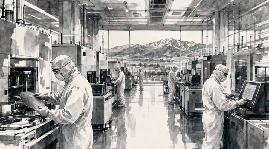
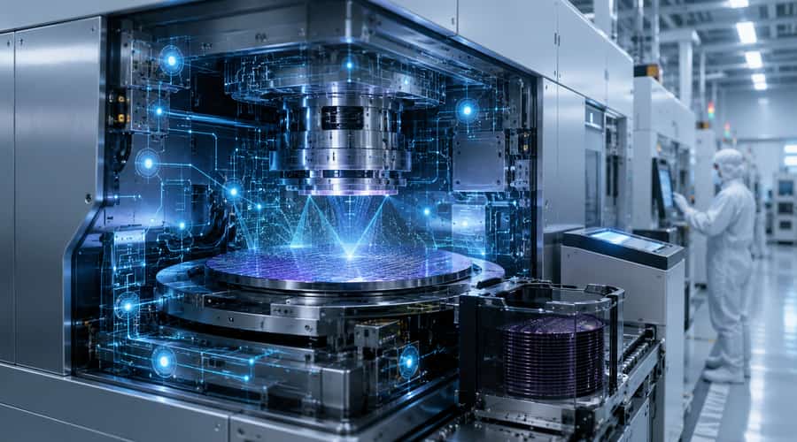
Semiconductor manufacturing has always been a game of small margins and expensive mistakes. A wafer can pass through dozens of process steps before a defect is fully understood, which means a problem caught late can waste time, materials, and capacity. Lam’s argument is that sensors placed closer to the action can feed AI models with the kind of real-time information that traditional inspection and offline analysis often miss.
Archer put it plainly in the Reuters interview: \"The more data you collect from the machine itself, or from the wafer, the better your models can be about predicting what’s happening and starting to really react to problems in the system.\" He also said AI can help identify conditions that engineers did not previously know were problems. That is the important part. The value is not only faster troubleshooting, but discovering weak signals before they become yield losses.
Lam has been building around that idea through both internal investment and startup partnerships. At a venture competition held at its Fremont headquarters, Lam Capital awarded a $250,000 investment to Lightfinder, an MIT spinout developing chip-scale spectrometers and imaging systems. The point of that kind of technology is to make measurement smaller, cheaper, and easier to place inside production environments rather than leaving it as a separate step.
If that approach works, fabs get a different operating model. Instead of sampling, waiting, and then adjusting, the machine can measure more often and feed richer data into models that help operators respond sooner. For customers such as TSMC, Samsung, Micron, and SK Hynix, even modest yield improvements can be meaningful because advanced chips and high-bandwidth memory are costly to manufacture and difficult to ramp.
Packaging is becoming part of the same race
Lam’s AI sensor push is also tied to a broader packaging problem. Advanced AI systems increasingly depend on dense combinations of logic, memory, and interconnects, not just a single leading-edge chip. That makes packaging more important, and it makes defects more painful because more value is packed into each finished component.
On May 20, Lam announced a Panel-Level Packaging Center of Excellence in Salzburg, Austria. The facility focuses on panel-level wet processing, where square or rectangular substrates can be used instead of traditional circular wafers. The attraction is simple: panels may allow more efficient use of surface area and better scalability for large, complex packages used in AI and high-performance computing.
This is not a side story. As advanced package designs get larger, older manufacturing assumptions start to strain. More chiplets, more memory stacks, and more complex interconnects create new places for defects to appear. A company that can measure those steps more precisely, and then use AI to understand the data, has a better chance of helping customers improve throughput without waiting years for a new process node to mature.
The US expansion signal
Lam is also positioning itself physically closer to the customers building in the United States. Archer said the company plans additional operations in Arizona and more investment around its Fremont, California headquarters. Real Estate Daily News reported in January that Lam bought a 147,638-square-foot building in north Phoenix for $45.77 million, near TSMC’s Arizona campus.
That location matters because the semiconductor supply chain is becoming more regional. TSMC is expanding in Arizona, Intel continues to invest in US manufacturing, and Samsung has been building out capacity in Texas. Equipment companies do not need to move everything next door, but proximity helps when customers are installing, tuning, and servicing some of the most complex machines in manufacturing.
For startups, the opportunity is more specific than \"AI for manufacturing.\" Lam’s strategy points to demand for specialized sensing, process analytics, metrology, simulation, and fab software that can fit into real production workflows. Lightfinder is one example of the type of company that could benefit. Others will need to prove they can survive the strict reliability, cleanliness, and integration demands of semiconductor fabs.
The next test is whether Lam can turn this roadmap into measurable yield gains for major customers. If the company’s sensor and AI upgrades help TSMC, Micron, or other chipmakers produce more usable silicon from the same equipment footprint, competitors such as Applied Materials and Tokyo Electron will have to respond quickly. The AI boom has already changed what chips are worth. Now it is changing the machines that make them.