IBM's 0.7nm nanostack work is a real semiconductor milestone, but you shouldn't mistake a research breakthrough for chips ready to flood AI data centers.
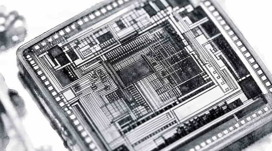
IBM has put a fresh number on the chip industry's old promise: smaller, denser, faster. According to Barron's, IBM Research announced on June 25, 2026, that it had produced what it describes as the world's first sub-1 nanometer chip technology, using a 0.7nm transistor node aimed squarely at artificial intelligence workloads.
The headline figure is the one you notice first. IBM says the technology could put nearly 100 billion transistors on a chip roughly the size of a fingernail. That is about twice the density IBM claimed for its 2nm research chip in 2021, the earlier breakthrough that helped push nanosheet transistor designs toward the leading foundries. The new design, called nanostack, takes that idea upward rather than simply shrinking it sideways.
This is not just a smaller label on a roadmap slide. IBM's nanostack architecture vertically stacks and staggers nanosheet-based transistors, giving engineers more room to tune different layers for performance and power draw. If you're running AI inference at scale, that distinction matters. The cost problem in inference is not only the price of the chip. It's the power, cooling, board space and memory movement that come with answering millions of prompts day after day.
Look at Nvidia and you can see why IBM is talking this way. Barron's noted that many current AI chips are still made on 5nm and 4nm processes, while Nvidia's Blackwell GPU uses a customized TSMC 4nm node. Nvidia's advantage is not only silicon density, of course. CUDA, supply, packaging and developer habit all sit around its chips like concrete. A better transistor design doesn't break that by itself.
But it does put pressure on the next round of AI hardware. If IBM's density and efficiency claims survive the long trip from lab wafer to commercial process, then chip designers get more room to make inference hardware smaller and less power-hungry. That is where the market is going. Training gets the attention, but inference is the bill that keeps arriving.
Frankly, the production gap is the story you should care about most. IBM does not manufacture advanced chips at commercial scale anymore, and MarketWatch pointed out that IBM doesn't currently sell microchips. This is a research announcement, not a foundry launch. IBM's 2nm work from 2021 was important, but it still needed partners and years of process development before it could show up in volume manufacturing.
Rapidus is the hard test
Rapidus is the obvious place to watch. The Japanese chipmaker is building its IIM-1 facility in Chitose, Hokkaido, and Tom's Hardware reported in February 2026 that it secured ¥250 billion, about $1.6 billion, from Japan's government and private backers including Sony, Toyota, SoftBank, Canon and Fujitsu. Its target is 2nm mass production in fiscal 2027, with IBM technology transfer at the center of the plan.
That sounds ambitious because it is. Tom's Hardware also reported that Rapidus has roughly 10 IBM engineers stationed on site and is in talks with more than 60 potential customers for chips used in AI, robotics and edge computing. Fujitsu is one of the names already circling the project, with a separate plan for a domestically made 1.4nm AI chip later in the decade. Those details give IBM's research work a possible route into real supply, not just conference-room admiration.
They also show the risk. Rapidus still has to prove it can turn advanced research into repeatable yield, and yield is where beautiful chip ideas often become expensive chip problems. A lab result can show the physics. A fab has to show the economics.
IBM is not working alone on the manufacturing problem. In March 2026, Tom's Hardware reported that IBM and Lam Research signed a five-year collaboration on High-NA EUV lithography and Lam's Aether dry resist technology, with the work based at IBM Research's Albany NanoTech complex in New York. That partnership is aimed at process flows for nanosheet and nanostack architectures, the unglamorous work that decides whether a node can be manufactured cleanly.
None of this makes Nvidia weaker tomorrow. It does make the AI silicon race less settled than it looked when the only question was how many Blackwell systems hyperscalers could buy. IBM has shown that sub-1nm logic is not science fiction. Now the harder work begins: getting that design out of Albany and into fabs that can build it by the wafer, not just prove it once.
Also read: Amazon raises its India bet to $48 billion as Big Tech turns the subcontinent into an AI proving ground • OpenAI quietly upgraded every free ChatGPT user to a smarter model and the competition should be worried • PropMIS Is Building HOA Management Software Where AI Was There From Day One